|
|
Microcontroller Interfacing |
|||
|
Due to my ladder logic compiler, I often get questions on how to build hardware to connect a micro to the outside world. I have not been able to find a good reference to suggest. Much of the material online is wrong or incomplete, or reflects good practice circa 1970. None of this is specific to a particular microcontroller or family of microcontrollers; it applies equally well to PICs or AVRs or 8051s or any other processor. Check the datasheet of your part to be sure, though, especially for things like how much current an I/O pin can drive. I use the phrases `GPIO' and `I/O pin' interchangeably; I just mean a pin on the microcontroller that can be configured as either a digital output or a digital input. (A typical micro has a lot of those.) It will presumably be clear from context whether the pin is configured as an input or an output. Also, I will assume that the micro is running from 5 V. Very little of this changes if it's not, though. I describe how to:
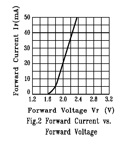
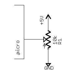
Light an LED from a Digital OutputThe LED is a two terminal device. We can therefore characterize it according to two quantities: the voltage across it, and the current through it. To a (fairly good) first order, the light output of the LED, either in photons per second or in milliwatts, is linearly proportional to the current through it. This means that it is useful to think of the LED as a current-operated device. (Of course, we could think about it as either; but there is a nice relation between the light output, which is what we ultimately care about, and the current; this is not true for the voltage.) To characterize a particular LED, we can apply a voltage (for example, using a DC power supply), and note the current through the LED (using an ammeter, or perhaps the ammeter built in to our power supply). We can repeat this for many different voltages, and plot these points to produce the LED's `V-I characteristics.' The manufacturer might have done this for us, and might provide this as a figure in the datasheet. Here I am reproducing that figure from the datasheet of a LITE-ON LTL-4223. This is a relatively typical red LED.
We can see that the relation between the LED's current and voltage is not very nice—it is not a straight line through the origin, or any other curve with a simple equation. Over the range of currents at which we expect to operate the LED (tens of mA), this curve is very steep. Going from a voltage of 2.0 V to 2.4 V, the voltage has increased by only 20%, but the current, which goes from 20 mA to about 50 mA, has more than doubled. That means that the current through the LED is very sensitive to the voltage across it. Equivalently, the voltage across the LED is very insensitive to (i.e., very close to constant with) the current through the device. This means that to a good approximation, we can model the LED as a constant voltage drop (and indeed, many manufacturers' datasheets do not bother with a curve, and quote only a single voltage). (If we wanted to model the LED's V-I characteristics more accurately, then we could do that as a series combination of an ideal diode and a resistor. The ideal diode has an exponential V-I characteristic; that is what is responsible for the non-linear part of the curve near 1.6 V. There is also an ohmic (i.e., linear relationship between V and I) resistance associated with the LED; the voltage dropped by that resistance is negligible at small currents, because V = IR is small when I is small, but becomes significant at higher currents. That is the reason why the curve shown above seems to approach a straight line at high current. But, we will hardly ever need that good of a model.) In any case, you already know that the circuit is this:
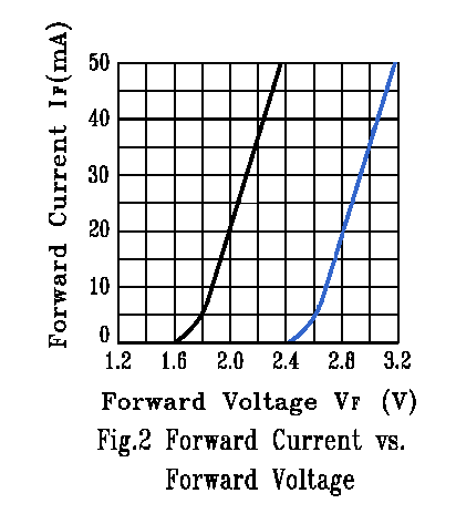
Sometimes the circuit is drawn backwards from the way that it is here, with the other end of the series circuit connected to +5V instead of ground. That was important for TTL (an old kind of logic), which could sink more current than it could source. For CMOS it does not matter. The micro's I/O pin is configured as an output. When it is driven low, zero volts appear across the series circuit, and no current flows. When it is driven high, 5 V appear across the series circuit. The LED drops about 2 volts; as we saw above, the voltage dropped by the LED is not very sensitive to the current through it, which means that we can get a very good approximation of the voltage dropped by the LED, even before we know the current through it. The resistor therefore drops 5 - 2 = 3 V, since the drop across the two series elements must total 5 V. This means that a current of I = V/R = 3/330 = 9 mA flows. We see from the datasheet that the LED is rated for a maximum continuous forward current of 30 mA, so we are well within the spec. We're not done, though. The LED's nominal voltage drop at 20 mA (or any current close to that) is 2.0 V, but we see from the datasheet (`Forward Voltage, Max.') that it could be as high as 2.6 V. This means that while the black curve below (which is identical to the black curve above) corresponds to a nominal device, a device whose V-I characteristics were described by the blue curve—or any curve lying between those two boundaries—would still meet the manufacturer's spec. If we got a worst-case LED that dropped 2.6 V, then the resistor would drop 5 - 2.6 = 2.4 V, and I = 2.4/330 = 7.3 mA would flow.
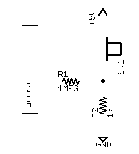
This is a noticeable change, a decrease of about 19%. Still, for this particular LED, and running from 5 V with this circuit, it's the best that we can do. If we could run from a larger supply voltage than 5 V, then the LED's voltage drop would be a smaller proportion of the total voltage drop in the circuit, so the current through the LED would be less sensitive to its voltage drop. It is also possible to use an active current source of some kind to make the current through the LED almost independent of its voltage drop, but that requires a more complicated circuit. This variation is the reason why it doesn't work at all to drive an LED with a constant voltage source. If we wanted to drive our minimum-drop (black curve) LED at 20 mA, then we see from the curve that we must apply exactly 2.0 V; but if instead we happened to get a maximum-drop (blue curve) LED, then we see from the curve that very close to zero current—so small that it is off the graph—would flow for any voltage less than 2.4 V. If we tried it the other way, and applied 2.6 V (to make sure that the maximum-drop LED lights up), then the minimum-drop LED will draw a very large current—again off the graph, but more than 50 mA—and the LED will overheat and be destroyed. The variation would not be a problem if we could watch the current through the LED as we slowly turned up the voltage, and set our constant voltage source to the particular voltage that produced the current that we wanted for that particular LED. This is what a current source does. This is also what the resistor does, although it doesn't do a very good job of it. If you omit the resistor (i.e., let it be a short circuit, zero ohms) from the circuit above, then in theory this corresponds to driving the LED from a five-volt voltage source. It seems from our discussion above that this should inevitably result in smoke. If you try this, however, then you will find that your circuit appears to work. This is because an I/O pin is not a perfectly stiff voltage source; it is the drain of a FET, which if you try to draw too much current looks a lot like a current source. The I/O pin itself limits the current, and if you measured the voltage at the I/O pin then you would find it to be much less than 5 V. This is almost certainly outside of the manufacturer's permitted operating conditions for the I/O pin, and is therefore not good practice. By the way, it's a little bit weird that the minimum voltage drop case for this LED is also the nominal voltage drop. It would be more common for the manufacturer to quote a minimum and maximum voltage drop, and a nominal (typical) voltage drop that is somewhere in between. A typical red or green LED drops about 2 volts. Blue LEDs drop more, typically around 3 volts. White LEDs—which are usually blue LEDs, with a phosphor that converts some of the blue to red and green—usually drop around 3 V. The voltage drop of an LED is related to the energy of the photons that it emits; shorter-wavelength (higher-energy) photons typically require a larger voltage drop. This is not always true; for example, certain `pure green' emitters have a larger voltage drop than you might expect from the wavelength of green. Read Switch Contacts with a Digital InputThis is very basic: you have a switch with two wires that are either open (switch open) or shorted (switch closed). This could be a pushbutton, or a magnetic reed switch, or a set of relay contacts. Do it like this:
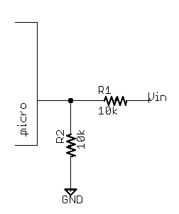
When the switch is open, R2 pulls the pin low through R1. When the switch is closed, the right side of R1 is shorted to +5V through the switch, pulling the pin high through R1. The resistor R1 is not strictly required. Its job is to protect the microcontroller. Without R1, if someone connected the switch terminals to a voltage greater than +5V or less than ground, the microcontroller would be destroyed. (See the next entry for why.) With R1, the excess voltage is dropped across the resistor, and as long as the resistor is big enough, the micro is unharmed. This also helps to protect against damage due to static discharge. With R1 = 1 MΩ (as shown), you can connect the input to 120 VAC with no damage. This is not recommended, of course. I chose R2 = 1 kΩ. If R2 gets too small, then a very large current flows through R2 when the switch is closed. This wastes power, and it might exceed the power rating of R2 (or the current rating of the switch!). If R2 gets too big, then it gets easier for random noise to pull the input pin high. Also, many switches are unreliable when the current through them is small—the current helps to clean the contacts when you switch. (It is also possible to draw this circuit backwards, with a resistor to +5V and a switch to ground. Historically, this was a better way of doing things, because TTL inputs did draw input current, and it took more current to pull them down than up. With CMOS inputs, this doesn't matter at all, so do it whichever way you like. Some micros might have internal pull-up resistors that you can enable (e.g. the AVRs), saving the need for external pull-up resistors, but the internal resistors might not be small enough to draw enough current through the switch for reliable operation.) Read a Digital Signal that Goes from 0 V (LOW) to 10 V (HIGH)The micro almost certainly takes standard CMOS logic levels: a logic LOW is around 0 V, and a logic HIGH is around 5 V (or whatever the micro's supply voltage is). If we had a digital signal that went between 0 V and 5 V, then we could connect it directly to a GPIO line on the micro. Of course, the micro does not require that the input level be exactly 0 V or exactly 5 V; they specify that anything less than some voltage (often, 0.2Vdd, or 1 V in this case) is LOW, and that anything greater than some voltage (often 0.8Vdd = 4 V) is HIGH. Since 0 V is less than 1 V, and 10 V is greater than 4 V, it seems like we can just connect our signal to an input pin, and everything will be fine. But if we do this, then the micro will be destroyed. This is because the micro is built with `protection diodes' on every pin; if the voltage on any pin exceeds the most positive supply voltage or is less than the most negative supply voltage (ground), then these diodes turn on and short that pin to the appropriate supply rail. The goal of this is to protect the chips against damage from electrostatic discharge (ESD, static electricity). In this case, however, if we apply our 10 V signal to the I/O pin of our micro running at 5 V, then the 10 V signal will be shorted to the 5 V supply rail. Depending on how much current our signal source (and the power supply) can provide, one or more of the micro, the signal source, or the power supply will be destroyed, as the 5 V supply and the 10 V signal fight it out. One simple way to fix this is to divide our 10 V signal's voltage by two, to make a 5 V signal. We can do this with a voltage divider:
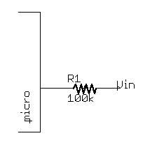
As Vin goes from 0 V to 10 V, the voltage at the I/O pin goes from 0 V to (10k/(10k + 10k))×10 = 5 V, so the micro is not destroyed, and everything works as designed. There are other ways of doing it, of course. The problem when we connected the signal source directly to the I/O pin is that we basically had two voltage sources shorted together through the protection diode: the signal source, at 10 V, and the 5 V supply. The effective `resistance' (V/I) of the diode (which is not constant, since a diode is not a resistor, but can be calculated at a particular current or voltage for any two-terminal part) is small, and there is some voltage across it, so a large current flows, forcing the part to dissipate a large power, and something smokes. If we connect the signal source through a large resistance, then the current is limited, and the problem goes away:
Here, for a 10 V input, the voltage at the pin is clamped to about 5 V (in fact, 5 V plus a diode drop, around 5.6 V). That means that a voltage of 10 - 5 = 5 V appears across the 100k resistor, so a current of about I = V/R = 50 μA flows. This is small, so nothing dissipates much power, and nothing overheats and burns. This is not very good practice, though. It is not just question of the heat dissipated by the protection diodes (although if you applied 10 V to an input directly, that alone might be enough to destroy the part). A fairly small (milliamps, or tens of milliamps) current through the protection diodes may put a chip into `latchup,' a state in which paths between the various silicon layers that are never supposed to turn on will conduct, draw a large current, and destroy the chip. Very few chips are rated for any current through the protection diodes, so if you use the micro this way then you are using it outside the manufacturer's specifications. Still, this circuit had an advantage over the voltage divider circuit. The voltage divider circuit works with the signal that it was designed for, but it will not work with a digital signal that goes from 0 V to 5 V. (The 0 V logic LOW produces 0 V at the pin, so that works, but the 5 V logic HIGH produces 2.5 V at the pin, which is not clearly low or high.) The circuit that relies on the protection diode still works fine with an 0 V to 5 V signal (or, for that matter, an 0 V to 20 V signal). We can design a circuit that will work with a logic level of 0 V (LOW), and anything greater than 5 V (HIGH), and still not violate the manufacturer's spec; we just have to provide the diode ourselves.
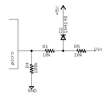
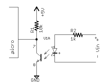
Here D1 clamps the voltage at its anode to a maximum of about 5 V. I specified a 1N4148, which is very common diode for low-current (tens of milliamps or less) applications. The 1N4148 is the old leaded part number, but similar parts in surface-mount packages (e.g. the MMBD4148) are available from many vendors. The voltage at the anode of D1 cannot exceed 5 + 0.7 V; so for an input voltage of 20 V, say, about 15 V are across the 10k resistor R5, and 1.5 mA flow. This is well within the rating of the diode. But, the maximum clamped voltage of 5.7 V at the anode of D1 still exceeds the manufacturer's absolute maximum input voltage rating for a micro running at 5 V (typically, they specify an absolute maximum input voltage of 5 V, or perhaps 5.3 V, because the protection diodes conduct only very slightly with just 0.3 V across them). R1 and R4 form a voltage divider to fix that. When the diode is conducting, its `dynamic impedance' (dV/dI, i.e. at the particular current at which the diode is operating, how much the voltage that it drops increases if you increase the current through it a tiny bit more) is very small. That means that R1 and R4 form a 10:11 (100k/(10k + 100k)) voltage divider, and this ratio is independent of R5. The 5.7 V clamped voltage gets scaled down to about 5.2 V, which the micro can tolerate with no problems. It would actually be more common to use a Schottky diode instead of our 1N4148, and omit the voltage divider (but keep the current-limiting resistor R5). A Schottky diode will conduct around 0.3 V, versus 0.6 V for a normal silicon diode. This guarantees that the external clamp diode will turn on well before the micro's protection diodes; so almost all the current flows through the clamp diode, and almost none flows through the protection diode. A typical small signal Schottky diode is the BAT54. Read (with Opto-Isolation) A Digital SignalAn opto-isolator allows you to transmit information between two circuits, without making an electrical connection between them. Instead, the information is transmitted as light. A typical opto-isolator will include an LED and a phototransistor, which are optically coupled together (i.e., the LED shines on the phototransistor). We can detect whether the LED is lit up by measuring the current through the phototransistor. Sometimes we might use these for safety; for example, if the signal comes in on a long wire that runs outside and we are worried that lightning might strike nearby, then perhaps the opto-isolator will be able to withstand the (hopefully, common-mode) voltage spike. Even if it is not, perhaps only the opto-isolator (and not the rest of the circuit) will be destroyed. Opto-isolators are also used just for convenience. Electricians accustomed to wiring up relays will find opto-isolated inputs very easy to deal with, because the interface is the same: you are given two wires, and the input is `on' when you apply a voltage across them. (PLC inputs are often opto-isolated, and it is probably more for that convenience than for safety.) You can use an opto-isolator like this:
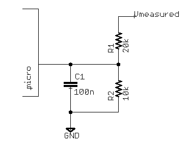
The opto-isolator here is an MCT62. This is a dual phototransistor-type opto-isolator, available in DIP and surface mount packages. Here I am using only one of the two channels. Almost any phototransistor-type opto-isolator would work. Notice that I do not show a connection to GND on the LED side of the opto-isolator. There is no need for any electrical connection between the two sides of the opto-isolator. This also means that the operation of the opto-isolator will be unaffected by any electrical connections that do exist between the two sides (for example, if for some reason there is a large voltage between the two different circuits' concepts of ground.) When zero volts are applied across the LED input circuit, no current flows through the LED. There is therefore zero photocurrent through the phototransistor, which permits R1 to pull the micro's input pin high. When a voltage is applied across the LED input circuit, the light from the LED causes a current through the collector of the phototransistor. This pulls the input pin low. For 0 V across the LED input circuit (Vin = 0 V), the LED is definitely off, so the micro input is definitely high. To determine the voltage at which the micro input goes low, we must refer to the MCT62's datasheet. When the micro input is LOW (at 0 V), there is a voltage of 5 V across the 10k resistor. This means that a current of 500 μA flows through the resistor, and therefore through the phototransistor. We refer to the MCT62's datasheet to determine its current transfer ratio, which is given as 100% at 5 mA and VCE = 5 V. This means that under those conditions, a current of 5 mA through the LED produces a photocurrent of 5 mA through the phototransistor. We are interested in what happens at 500 μA, though. From the `Normalized CTR vs. Forward Current (Normalized to IF = 10 mA)' figure, we see that the CTR is up to a factor of almost 1.2 at 5 mA, and down by a factor of about 0.6 at 500 μA. This means that we are down by a factor of 0.6/1.2 = 0.5 from the CTR at 5 mA, for a CTR of 50%. So, we need a current of at least (500 μA)/(50%), or 1 mA, through the LED to guarantee that the phototransistor can pull the input pin low through the 10k resistor. The LED drops at most 1.5 V at 20 mA—and presumably less, but we don't know how much less, at 1 mA—and the 1k resistor at 1 mA drops 1 V. This means that we need at least 1 + 1.5 = 2.5 V across the input circuit to guarantee that we can detect this (i.e., that the micro's I/O pin goes LOW). The maximum tolerable input voltage is determined by the maximum current that the LED can tolerate. This is given as 60 mA, so a maximum input of 1.5 V + (60 mA)×(1k) = 61.5 V will stay within that spec. Note that at 60 mA, R2 dissipates I2R = 3.6 W! A resistor capable of handling that much power without burning up will present a surface area of at least a few square centimeters. In practice I would not trust this circuit at either the minimum or maximum input voltage; something like 5 to 30 V seems like a more comfortable range. On the low side, the CTRs that I used were all at a VCE of 5 V, so I would like to leave some slop in case the CTR is much lower at smaller VCE. (We are aiming to saturate the transistor, but they made their measurements at a particular point in the active region, so the numbers might not be quite the same.) On the high side, I would rather not pay for a five watt resistor for R2; 30 V gives less than 1 W in R2, which is more reasonable. Measure a DC Voltage Between 0 V and 15 VMany microcontrollers have A/D (analog-to-digital) converters. These map a voltage at an input pin on to an integer. A ten-bit converter is typical; that means that it maps the smallest voltage on to the integer 0, and the largest on to 1023 (i.e, 210 - 1). The `smallest' voltage is usually ground. You can almost always configure the `largest' voltage to be the positive supply voltage, which in this case is +5V. Your +5V supply is probably regulated, and thus accurate to within a few percent, so that is probably an easy way to hook things up. So in this case, we can measure a voltage between 0 and 5 V, but we have a voltage between 0 and 15 V. The easiest way to fix this is with a voltage divider:
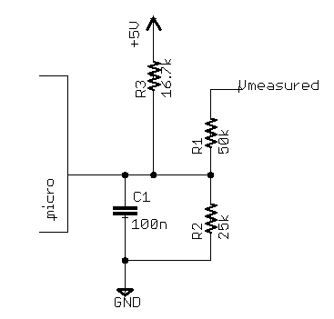
This multiplies the incoming voltage by a factor of R2/(R1 + R2). In this case that is 10k/(10k + 20k), or 1/3. The capacitor helps to reduce high-frequency noise. An ADC reading of 0 corresponds to 0 V. An ADC reading of 1023 corresponds to 15 V. It is linear in between (so that an ADC reading of 512 is about 7.5 V). If you make the resistors very large, then noise becomes a problem. If you make the resistors very small, then they draw a lot of current from the voltage source that you are measuring, which might load it down. (The load that the source sees is (R1 + R2); make sure that it is rated for that, or measure it with a multimeter to make sure that its voltage does not go down when you connect it to your circuit). Do not measure very high (>50 V, say) voltages this way; it is not safe. This works with AC voltages, but maybe not how you expect—you measure the value of the AC voltage at a particular moment in time, not the RMS or peak voltage. Measure a DC Voltage Between -15 V and 15 VThis is a little bit trickier. We don't just want to multiply the voltage by a constant, like last time (since R2/(R1 + R2) times -15 V is always going to be negative, no matter what we do, and we can't measure negative voltages). This time we want to shift it as well:
This produces a voltage Vadc = (Vmeasured + 15)/6, which means that Vadc goes from 0 to 5 V as Vmeasured goes from -15 to +15 V, which is what we want. You can design this for any range that you need, by choosing appropriate resistor values. One way to do so is to write KCL at the microcontroller pin. The pin itself draws zero current, because it is an input, and the capacitor draws zero current at DC. The math will turn out easier if we use conductances instead of resistances, so let G1 = 1/R1, G2 = 1/R2, and G3 = 1/R3. The KCL gives
(Vadc - 5)/R3 + (Vadc - Vmeasured)/R1 + Vadc/R2 = 0 This is a weighted average, where the contribution of each voltage (+5V, Vmeasured, or ground = 0 V) is weighted by the conductance of the resistor connecting it to the I/O pin. A higher conductance (equivalent to a lower resistance) means that it influences the voltage at the I/O pin more, which makes sense. We want to map our input voltage, which goes from -15 V to +15 V, so that it goes from 0 V to 5 V. As we said above, this means that we want
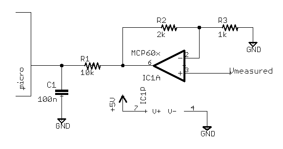
Vadc = (Vmeasured + 15)/6 So let G1/(G1 + G2 + G3) = 1/6, and let (G3/(G1 + G2 + G3))×5 = 2.5, and solve. This is two equations in three variables, so you have one extra degree of freedom. That means that you can choose one of the variables arbitrarily, and solve for the other two. For example, you could choose R1 = 50kΩ, which gives G1 = 20 μΩ-1, and solve for G2 and G3. Of course that's not how I actually picked those values. I know how to shift a voltage between -5 V and +5 V so that it's between 0 V and 5 V: I just have to make a voltage divider between that voltage and +5 V, with equal resistors. This will weight the two inputs (+5 V, and the signal being measured) equally, so the output voltage will swing between (5 + 5)/2 = 5 V and (5 - 5)/2 = 0 V, like I want. So, all that I had to do was transform the input voltage, which goes between -15 and +15 V, so that it goes between +5 and -5 V, and then I wouldn't be done, but I would know what to do. I can do this with a voltage divider: ±15×(R2/(R1 + R2)) = ±15×(25/(25 + 50)) = ±5. The R1/(R1 + R2) voltage divider has an output resistance of R1 in parallel with R2; think about the Thevenin equivalent circuit if that isn't clear. I therefore chose R3 equal to R1 and R2 in parallel, or R3 = 1/(1/R1 + 1/R2). This is much faster than solving simultaneous equations; you can do it in your head. Thevenin equivalents are a good tool for solving the kinds of circuits that people actually build. Measure a DC Voltage Between 0 V and 1.7 VThe microcontroller's A/D can measure a voltage between 0 V and 5 V. That means that we could connect this voltage straight to an A/D input, and we're done, because a voltage between 0 V and 1.7 V is also between 0 V and 5 V. This is wasteful, however. Of the 1024 possible codes that a 10-bit A/D converter can produce, only 342 ((1.7/5)×1024) will actually occur. That means that we are throwing away between one and two bits of resolution. The solution is to buffer and amplify the input signal before connecting it to the A/D converter, and we can do this with an opamp:
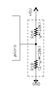
The opamp is configured as a non-inverting amplifier, with a gain of (1 + 2k/1k) = 3. This means that as the input Vmeasured goes from 0 V to 1.7 V, the output goes from 0 V to 3×1.7 = 5 V. Any gain of less than a hundred is easily achieved with this circuit. For larger gains, nonidealities of the opamp (its `input offset voltage', and for fast signals its gain-bandwidth product) may no longer be negligible. I have specified an MCP60x, where x is 1 (single opamp), 2 (dual, two opamps in one package), or 4 (quad). This is a modern CMOS opamp from Microchip. The pin numbers shown on the schematic are for the single in a plastic DIP package, but you get the same amplifier whether you buy them in singles, duals or quads. It is cheap; the single in PDIP costs forty cents from Digikey in quantity ten. It is `rail to rail output,' which means that it can produce an output voltage very close to either the negative (0 V) or positive (5 V) supply. (Of course, it cannot produce an output voltage more negative than its negative supply, or more positive than its positive supply. This is true for almost any IC.) Working with slow (< 1 kHz) signals, for small gains, and with reasonable (between 330 Ω and 1 MΩ, say) resistor values, an MCP60x will be within tens of millivolts of an ideal opamp, as long as you keep the output voltage within the limits of the supply. This amplifier (and many comparable parts from Microchip and its competitors) is better in every way than any comparably-priced part from twenty years ago. In particular, the often-discussed 741 is now of mostly historical interest. Measure the Position of a PotentiometerA potentiometer is a variable resistor. You can change the value of the resistor by turning a knob, or by moving a slider back and forth. Sometimes these are used as human interface devices, for example when you turn the volume knob on a radio, or slide a dimmer switch to turn on the lights. It's also possible to arrange things so that some machine part actuates the pot. For example, you could attach a float at the end of a long stick to the shaft of a rotary pot, and use it to measure the liquid level in a tank. If you take a look at a pot, then you will see that it has three terminals, not just two, as a normal resistor does. This is because the pot actually consists of two resistors, configured as a voltage (or potential, hence the name) divider. In concept, a 10k pot looks like this:
The pot is represented by R1A and R1B. They are internally wired in series. The point where R1A and R1B connect is called the `center tap,' or the `wiper.' Here, I have shown that the center tap of the pot is connected to an A/D input pin on the microprocessor. The other two terminals of the pot are connected to +5V and to ground. The variable y represents the position of the pot; it goes from 0 to 1. As y increases, R1A gets bigger and R1B gets smaller, but their sum stays constant at 10k. That is why this is called a 10k pot. When the pot is turned all the way in one direction (counter-clockwise, let's say), y is equal to 0. This means that the center tap is shorted to +5V, through R1A = 0×10k = 0 Ω. When the pot is turned all the way clockwise, y = 1, and the center tap is shorted to ground through R1B = 0 Ω. In between, the voltage at the center tap is a linear function of y. For example, when y = 0.5, the center tap looks like a voltage divider, with 5k to ground and 5k to +5 V, so the voltage at the center tap is 2.5 V, or 0.5×(5 V). So, if you want to use a microcontroller to read a potentiometer, do this:
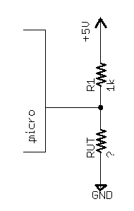
The voltage at the microcontroller pin will go from 0 V to 5 V as the user (or the machine, or whatever) turns the pot. The A/D can convert this voltage into an integer in your program. I specified a 10k pot here. This is a very common value. The `output resistance' of the circuit driving the A/D pin must be smaller than some limit, or else the A/D will not be accurate. This limit is typically given in the electrical specifications in the microcontroller's datasheet. The requirement comes about because the input of a typical A/D looks like a capacitor. That capacitor, in combination with our output resistance, gives an RC time constant, and we have to make sure that the low-pass filter that we have accidentally created has settled to within an LSb before the A/D starts its conversion. That means that we can tolerate bigger output resistances if we slow down the A/D converter, and most micros provide some register where you can do that. (There is actually still an upper limit, no matter how slow you run the converter, because of leakage currents, but that's not usually an issue. Even if the manufacturer quotes some maximum tolerable output resistance due to leakage currents, that limit is over the full specified temperature range, and the leakage current will be much smaller if you're using the parts around room temperature.) Here, the output resistance will change as a function of the position of the pot, but it will never be more than 10k/4 = 2.5k. (This happens when y = 0.5, i.e. the pot is in the middle of its range. At that point, the Thevenin equivalent resistance of the pot is two 5k resistors in parallel, or 2.5k. When y = 0 or y = 1, the output resistance is zero.) That will almost certainly be fine, though you would have to check the datasheet for your microcontroller's A/D to be sure of that. Everything that I said above is true only for a `linear taper pot,' but most pots are linear taper. It is also possible to buy pots where the logarithm of the variable y is proportional to the position of the slider. These `log taper pots' are typically used in audio applications, where perceived (by the human ear) loudness is a function of the logarithm of the actual signal level, in volts applied to the speaker. Measure an Unknown ResistanceA lot of sensors look like resistors. For example, a photocell is a resistor whose value is determined by the amount of light that is falling on it. A strain gauge is a resistor whose value is determined by the strain in the material that it is attached to. A load cell is a strain gauge attached to a spring, so it is a resistor whose value is determined by the weight of whatever is sitting on it, like you would use in an electronic balance. A thermistor is a resistor whose value is determined by its temperature. A potentiometer is also a sensor that looks like a resistor, but it is special, because it has three terminals, not two. You could use only two of those terminals, and the methods described here would still work fine, but it's better to use the method described in the section above this one, because that method is more linear. That method will therefore make better use of your A/D's dynamic range (i.e., give you more bits of useful resolution) in most applications. Let's say that we have some arbitrary resistive sensor, whose resistance varies from 500 ohms to 5k. We want to measure its resistance using the microcontroller's A/D. We can do this by making a voltage divider, where one of the resistors is known, and the other is the one that we're trying to measure:
Here, R1 is a fixed 1k resistor. RUT is the resistor under test, the sensor. This is a voltage divider, so the voltage at the micro pin is given by Vadc = (5 V)×RUT/(RUT + 1k) Solving for RUT, we get RUT = Vadc×(1k)/[(5 V) - Vadc] This isn't a very nice equation, but the microcontroller can do the math. Be careful how you code it, though. It's best to always use integer math, for speed, but if you do then you have to make sure that nothing overflows or underflows. Working in C, I would write that equation as // I assume that you have made appropriate typedefs for unsigned_int16 and // for unsigned_int32; these will vary from compiler to compiler. unsigned_int16 adc_val; unsigned_int16 RUT; unsigned_int32 temp; adc_val = read_adc(); // i.e., however you do it with your micro // I assume that 0 V corresponds to adc_val == 0, and 5 V to adc_val == 1023. temp = adc_val; temp = 1000*temp; RUT = temp/(1024 - adc_val); Notice that I used a 32-bit temporary variable, because 1000×adc_val could be as much as 1023×1000, which would overflow a 16-bit integer. Also notice that I did the multiply before I did the divide, to make sure that I didn't end up with any intermediate results less than one. I cheated slightly, specifying 1024 instead of 1023, so that this code will never divide by zero. This introduces only a very small error. I am also ignoring the rounding error, which is present because division in C truncates. For RUT = 500 Ω (lower limit), Vadc = 1.667 V. If we assume a reference voltage of 5 V and a ten-bit A/D, then this corresponds to an ADC code of (1.667 V)×[1023/(5 V)] = 341. For RUT = 5k, the ADC code is 852. This means that we are using only (1+852-341)/1024 = 1/2 of our available A/D codes. We are throwing away some of our dynamic range, but not a huge amount. The codes are not uniformly distributed along our 5k - 500 = 4500 ohm range, though. For example, here is a table of ADC codes and corresponding resistances near 500 ohms. The ADC code is in units of least significant bits, or LSbs. adc_val=342 RUT=501 adc_val=343 RUT=503 adc_val=344 RUT=505 adc_val=345 RUT=508 adc_val=346 RUT=510 The measured resistance is changing at a rate of 2 or 3 ohms/LSb, so we can make measurements with a resolution of two or three ohms. Now look at the codes and resistances near 5k ohms: adc_val=850 RUT=4885 adc_val=851 RUT=4919 adc_val=852 RUT=4953 adc_val=853 RUT=4988 adc_val=854 RUT=5023 The measured resistance is now changing at a rate of about 30 ohms/LSb, so we are measuring with a resolution of about thirty ohms. This is one tenth the resolution as before. That means that while we could easily distinguish the ten-ohm change between RUT = 500 Ω and RUT = 510 Ω (4 LSbs), we could not distinguish the ten-ohm change between RUT = 4.990k and RUT = 5.000k (less than 1 LSb). This is because the relationship between the measured resistance and the voltage at the A/D input is non-linear. That might be okay, though, or even desirable. For example, we can distinguish the 2% change between RUT = 500 Ω and RUT = 510 Ω (4 LSbs) just as easily, more or less, as the 2% change between RUT = 4.90k and RUT = 5.00k (4 LSbs). If we are interested in relative differences, and not absolute differences, then the non-linearity of our measurement technique is actually helpful. (Let x be the ADC code, and let R be the resistance under test. To distinguish any absolute difference in R as well as any other, we should have dx = k(dR), or dx/dR = k, or x(R) = kR + C, where k and C are arbitrary constants. That's a line. To distinguish any relative difference in R as well as any other, we should have dx = k(dR/R), or dx/dR = k/R, or x(R) = k(ln(R)) + C. That's not the transfer function that we have here—we have something of the form x(R) = kR/(R+ 1) + C—but you can show that ln(R) is approximately equal to 4R/(1 + R) - 2 when R is close to 1; look at the first few terms of the Taylor expansion for each function about that point, or just plot them, with the R-axis log-scale.) If the non-linearity is a problem, then we could modify our circuit so that the voltage at the A/D is a linear function of the measured resistance. One way to do that would be to drive a constant current through the resistor under test, and measure the voltage across it, which will be given by Ohm's law, V = IR. That would require more components, though. Measure a TemperatureUse an analog temperature sensor like an LM135, LM235, or LM335. These produce a voltage proportional to the absolute temperature (in Kelvins). Just measure that voltage directly using an A/D, and you can measure temperatures between -40 and 100 degrees Celsius to within a few degrees:
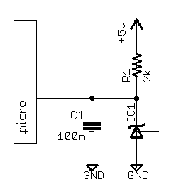
The LMx35 parts will drop a voltage very close to 10 mV/Kelvin. If we assume that the A/D's voltage reference is 5 V, then that means that the temperature in Kelvin is given by (ADCREG×500/1023), where ADCREG is the register that reports the 10-bit A/D result. The symbol that I drew for the LMx35 looks like a Zener diode. This is not because the design of these parts involves a Zener diode in any way; it is just common practice for parts that are used in the same way that a Zener diode would be (apply a poorly-controlled current through the device, and the output is the voltage drop across the device). The datsheet specifies that the temperature sensor may be run at any current between 400 μA and 5 mA. By design, the output voltage will be relatively insensitive to the bias current. I chose to run the device at approximately 1 mA. We have 5 V (our supply voltage) to drop total; room temperature is around 300 K, so the part will drop around (300 K)×(10 mV/K) = 3 V, leaving 2 V to be dropped by the resistor. At 1 mA, this requires a 2k resistor. (Of course, the bias current will change with the temperature; but as long as it stays between 400 μA and 5 mA, everything should be fine.). We are not using our A/D's dynamic range very effectively here. If the temperatures that we measure go from -30 to +70 Celsius, then that is a span of only 100 K, or 1 V. The A/D measures a voltage span of 5 V, so we are throwing away four fifths of our dynamic range. We could fix this with an opamp, but it is probably not necessary—with just this simple circuit, we can measure the output voltage accurately enough that the accuracy of the temperature sensor, and not the accuracy of our A/D, is what limits our accuracy overall. C1 helps to reduce noise, but it can be omitted. With or without C1, it is probably a good idea to take many (around 32, say) A/D readings and average them together. This also helps to reduce noise, which is important when you are trying to measure small changes in voltage. (A degree is roughly 2 LSb, for a 10-bit converter with a 5 V reference, so you will not be able to measure to within a degree unless you are getting almost the full A/D converter resolution.) I left the ADJ terminal of the LMx35 open. This terminal can be used (as shown in the datasheet) to calibrate the device, using a variable resistor. If you are reading the sensor with a micro, however, then it is probably easier to apply any calibration curve required in software. If you need to measure a broader range of temperature (very hot or very cold), then probably something like a platinum resistive sensor is appropriate. These are more difficult to interface to. Output Characters on an LCDUse a serial LCD, like the ones from Crystalfontz. You only have to hook up three wires: power, ground, and the TX line from the micro's UART. These are very easy to use. Parallel LCDs (which use a controller IC like the ubiquitous HD44780) are much cheaper—indeed, a serial LCD is usually just a parallel LCD that comes with a processor to do the serial-to-parallel conversion. They are more difficult to use, however, and you will need to connect more wires. Switch a 100 mA, 10 V LoadThe GPIO pins are usually rated for around 20 mA, so this is a little bit too much to switch directly from the micro. The solution is to add a transistor:
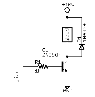
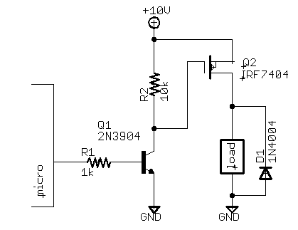
The I/O pin is configured as an output. When the I/O pin is low, no current flows through the base of the transistor Q1, so no current flows through the collector and the load. When the I/O pin is high, roughly (5 - 0.7) V appear across R1, so about 4.3 mA flow in to the base of the transistor. The datasheet specifies a minimum beta of 30 at 100 mA, so the transistor wants to turn on until at least 30×4.3 = 129 mA flow through the collector. Our load draws less than that, so the transistor will just turn on all the way, like a switch. (In fact, it will drop a small voltage VCEsat, a few hundred millivolts.) This is the best way to switch a small motor, or a solenoid, or a light bulb, or any similar load. I used a 2N3904, which is a very common NPN transistor. This is a very old through-hole part, but surface-mount parts with similar specifications (e.g. an MBT3904) are easily available. The transistor is useful up to about 100 mA of load current. The diode D1 protects the transistor if you are switching an inductive load (like a solenoid, or a motor, or anything with a lot of wire coiled up). An inductive load stores energy, and when you turn it off, that energy has to go somewhere. Without the diode, the energy can produce a very large voltage at the collector of Q1 and destroy the transistor. With the diode, this energy is harmlessly dissipated in D1 (and the load) as heat. I specified a 1N4004 diode. The 1N400x series is a very popular series of power diodes. The last digit determines the voltage rating. Switch a 1 A, 10 V Load That Always Stays Connected to GroundIn the previous example, we always left the load connected to the positive supply, and we connected and disconnected the ground lead. If that is okay, then it's usually the best way of doing things. (It happens due to the device physics that it's easier to make low-side switches than high-side switches.) But, if the device has any other connection to ground, then it will just never turn off. For example, imagine that your load is a motor whose metal case is tied to its negative supply terminal. If that motor is bolted to a metal frame to which your supply is grounded, then the motor will never turn off with the previous circuit. We try to turn it off by disconnecting the ground wire, but it still has a perfectly good ground through the case and the metal frame. So instead of disconnecting the negative wire, we want to disconnect the positive wire. Do it like this:
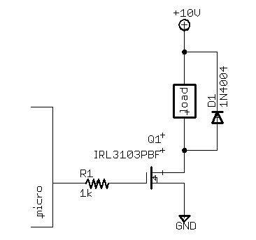
I am using a p-FET now, instead of the NPN BJT in the previous example. Q2 does the actual switching; Q1 is just there to generate the correct voltage levels to drive Q2's gate. When the I/O pin is low, no current flows through the base of Q1, so no current flows through the collector of Q1. That means that R2 drops no voltage, so the gate of Q2 is around 10 V. That means that Q2—and the load—is off. (This is a p-FET, not an n-FET, so everything is backwards; the more positive gate voltage turns the transistor off, and the more negative one turns it on.) When the I/O pin is high, the BJT conducts, so it pulls the gate of Q2 near ground. That turns Q2 on, applying power to the load. For the gate-drive circuit, I specified another 2N3904, because those are very cheap. I have specified an IRF7404 p-FET. This is not quite as standard as the other parts that I have been using, but it is cheap, and it seems to be fairly available at this time. The diode does the same job as before, and can be omitted for a non-inductive load. Switch a 10 A, 40 V LoadThis is too much for our 2N3904. We could get a big power BJT (bipolar junction transistor), but then we would have to drive a lot of current through its base to turn it on, because the current through its collector would be so huge. We could try a Darlington BJT, which uses two transistors to deliver twice (β2) the current gain, but a FET will probably give better performance—less power dissipated in the switch for a similarly-priced part, and faster switching—than the BJT. The FET is easy to use, because the gate draws no DC current. In theory, we can switch as many amps as we would like just by changing the gate voltage with our I/O pin. The circuit looks like this:
The concept is the same as when we used an NPN transistor. The resistor doesn't actually do anything at DC, because (unlike the NPN transistor's base) the n-FET's gate does not draw any current. The resistor helps to protect the micro from transients when the high current switches, though. I specified an IRL3103PBF for the FET. I chose this FET because it will operate from a small voltage swing on the gate. Traditionally, power n-FETs were designed to operate with a voltage of 0 V (off) or 10 V (on) at the gate. We need something that will turn on fully from a much smaller voltage, so I chose a `logic-level FET,' which is more or less fully on with 5 V on the gate. Notice that we didn't have to choose a logic-level FET for the previous circuit with the p-FET. There, the gate swung between 0 V and 10 V, so we had plenty of gate voltage swing. It is because we are driving the gate directly here that we have to choose a bit more carefully. In fact, we could use a similar circuit with a 2N3904 to produce an 0 to 10 V gate voltage swing if we needed to, but it is easier to choose a logic-level FET. The diode does the same job as before, and can be omitted for a non-inductive load. We could probably live without it regardless; the FET that we are using is rated for avalanche breakdown. If the drain-source voltage of any FET is brought past the rated VDSmax, then the FET will conduct from its drain to its source, independent of its gate voltage. In general this is bad, and may result in permanent damage to the part. The datasheet for the IRL3103 explicitly permits this mode of operation, though, and we can therefore take advantage of this. Switch a 120 VAC LoadUse a mechanical relay. To drive the relay coil, use a single 2N3904 transistor, as shown above. Nov 2006, Cambridge MA |